
I (believe I) am making good progress on designing the TTL CPU. Most of the actual CPU design is relatively stable now, and bug discoveries in the hardware design are infrequent, so now I get to move up a level and work on the instruction set. After that, it's just the bootloader, operating system, and application software. Oh, and the small matter of the physical hardware assembly...
While trying to get the CPU executing code correctly in the test harness, I spent most of a day solving problem-after-problem that each ultimately came down to "the carry flag is set when I didn't expect it". It turns out that having the carry input enabled by default was way more of a footgun than even I predicted. I briefly considered adding a control bit to enable it where wanted, but decided it was simpler just to get rid.
My original intention for the carry flag was that it would make it easier to write code that does arithmetic with values wider than 16 bits, but this is possible even without a carry input, and personally I have never used a carry flag in my life, so I don't think I'll miss it (mostly because it's not exposed in C, and my mind works like C).
Following the tradition of computers named with contrived backronyms, I'm thinking of calling the computer "SCAMP", for something like "Simple Computing and Arithmetic Microcoded Processor". But I'm interested in better, so let me know if you think of something.
Goals
The goals of instruction set design, for me, are:
- It should be easy to guess which instructions are available without consulting the documentation
- It should not be needlessly difficult to write programs
- Common operations should be fast
There is some tension here, because one way to make common operations fast is to make non-orthogonal instructions that do quite specific things, but that then makes it harder to predict which specific addressing modes are available for which instructions.
I'm not sure I've done a particularly good job of meeting any of these goals, but I also don't think I could do a lot better, given the limitations of the hardware design.
Documentation
Even though I've invented the instruction set myself, I find good documentation crucial. Trying to write assembly language without a decent reference is an exercise in frustration.
The best assembly language reference I have ever used is the clrhome Z80 instruction set table. It has a 16x16 grid showing every 1-byte opcode at a glance, with more information available when you hover over a particular instruction.
I have copied the style in my own instruction set cheatsheet:
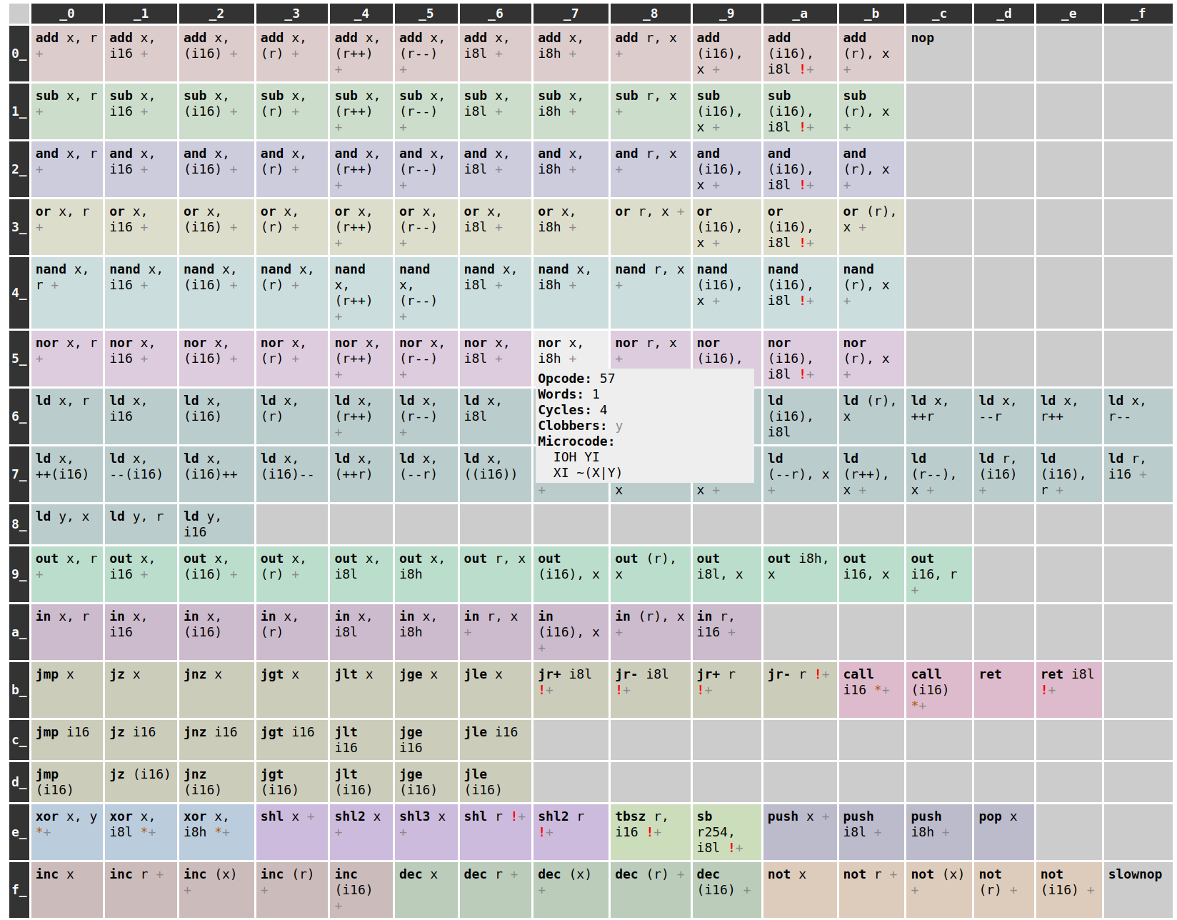
I also used coloured cells to visually group similar instructions together. Initially I was planning to do the hover effect with JavaScript, but it's surprisingly easy to do with pure CSS.
You can kind of view parts of the instruction table as a "periodic table of instructions", which makes it easy to tell if some obvious orthogonality is missing (for example, if an addressing mode exists for and but not sub, then the rows won't match). I've tried to lay it out in a way that naturally lends itself to adding extra addressing modes to existing instructions without disturbing the rest of the layout, but it's relatively likely that at least some of the opcodes will change.
The instructions are implemented with microcode, and the instruction set cheatsheet is generated automatically from the microcode source, via an intermediate instructions.json file which describes the instruction set.
instructions.json is also used to configure the assembler. This way, whenever I make a change to the instruction set (including adding/removing instructions, or moving around existing instructions), it is automatically reflected in the assembler and the documentation with no code changes required. This gives me good confidence that the assembler is always generating the correct opcodes, and that the documentation always matches, which removes a big source of problems.
I also decided to include the microcode implementing each instruction in the hover popup on the cheatsheet. This way, if (ha) I have written any microcode bugs, I have half a chance of debugging the microcode by accident while trying to debug the program. It also might be useful in case I have any doubts about how an instruction works.
Pseudo-registers
One of the peculiar features of my CPU is that it has a mechanism for putting the low bits of the instruction word on the bus, but with the upper bus bits set to 1. This allows instructions to use the low 8 bits of the instruction word to reference an address in the top 256 addresses of memory.
To keep things simple, the CPU has a serious shortage of real registers: it has the bare minimum of registers required to be able to give 2 operands to the ALU. Namely, 2.
2 registers is not enough to do anything interesting with, so intermediate values will have to go out to memory.
It would be really inconvenient to have to manually pick global addresses for all intermediate values, so I've given the assembler a special syntax for referring to addresses in the top 256 words. They're called "pseudo-registers" and are called r0 to r255. This is similar to an idea from Nand2Tetris, where the first 16 words are referred to as R0 to R15, except I couldn't put my pseudo-registers in the first 256 words, because the first 256 words are backed by ROM.
I'm using r255 as a stack pointer, and there are dedicated instructions that use it this way, and r254 for various purposes, as we'll see below.
In the instruction set cheatsheet, an r operand is just syntactic sugar for an (i8h) operand, i.e. an address in the top 256 words, indexed by the low 8 bits of the instruction word.
Microcode
The microcode source is in ucode/ucode.s in the github repo, with documentation in doc/UCODE.md.
Currently I am manually implementing every single instruction, although it might be better to write a program to generate the microcode source from a more high-level description. For example, add, sub, and, or, nand, and nor each currently support exactly the same addressing modes and differ only by the ALU operation that they select. This is an obvious candidate for writing a program to generate all the different versions, instead of maintaining them manually.
Here is a selection of instruction implementations, to give you a flavour of how the microcode works. Note that things like Y-1 are syntactic sugar in uasm for setting the ALU control bits. There is not a general mechanism to compute arbitrary arithmetic. Y-1 is just NX EY F. I have written up an ALU reference.
add x, i8l:
    IOL YI  # Put the low 8 bits of the instruction word (called i8l) on the bus, and load the bus into y
    XI X+Y  # Use the ALU to put x+y on the bus, and load the bus into x
Should be self-explanatory.
push x:
    -1 AI   # Use the ALU to put -1 (0xffff) on the bus, and load it into the address register
    MO YI   # Put M[0xffff] on the bus, and load it into y
    MO AI   # Put M[0xffff] on the bus, and load it into the address register
    MI XO   # Put x on the bus, and load it into M[M[0xffff]]
    -1 AI   # Use the ALU to put -1 (0xffff) on the bus, and load it into the address register
Y-1 MI # Put Y-1 on the bus, and load it into M[0xffff]M[0xffff], aka r255, aka sp, is the stack pointer. The microcode dereferences the stack pointer, stores x at the address the sp points to, then writes sp-1 into sp. (The stack grows downwards).
tbsz r, i16:
    IOH AI     # Put i8h in the address register
    MO XI      # Load from (i8h) into x
    PO AI      # Load program counter (currently pointing at the i16) into the address register
    MO YI P+   # Load the i16 into y and increment PC
    X&Y        # Compute X&Y with the ALU, discard the result, and just use it to set the flags
    PO JNZ P+  # Put the PC on the bus, jump if flags register says "not zero", increment PC
This instruction boils down to "skip the next 1-word instruction if r & i16 is zero". Mostly it might be easy to follow, but the final step is confusing. The part to understand is that the JMP input to the program counter has higher priority than P+. JMP is computed by combining the jump flags with the flags register, in this case JNZ means JMP will be enabled if the Z bit is not set. So in the event that Z is set, P+ applies and we skip the next instruction, but in the event that Z is not set, the JMP means the PC loads its output back in, so the P+ bit has no effect. Quite tricksy.
xor x, y:
    -2 AI      # Set address register to 0xfffe
    MI X|Y     # Set r254 = X|Y
    YI ~(X&Y)  # Set Y = ~(X&Y)
    MO XI      # Set X = r254
    XI X&Y     # Set X = X&Y
This computes x^y == (x|y) & ~(x&y) ("x or y, but not both"), using r254 as scratch space.
Weirdness
The instruction set I'm using at the moment has quite a lot of weirdness unfortunately, but it all makes sense if you understand the underlying limitations, which are:
- The sequencer only counts from 0 to 7.
- There are only 2 general-purpose registers.
- The ALU can only generate constants 1, 0, -1, and -2.
- xor and bitwise-shift-right are not natively supported by the ALU, and are achieved through funny tricks.
Instructions conspicuous by their absence
The first 2 steps of microcode for every instruction are just loading the program counter into the address register, and then loading the instruction word into the instruction register. That leaves 6 clock cycles available for actual operations. Any operations that need more than 6 cycles can not be implemented with a single instruction.
It would be natural for the existing instruction set to also include push r, pop r, xor x, r, add x, (++r), and shl3 r (bitwise shift-left by 3 on a pseudo-register, currently shl3 only exists for x). Unfortunately these would all go over the cycle limit, so they just have to be excluded.
In principle I could add another bit to the sequencer so that it counts from 0 to 15, but the microcode addressing is not very flexible, so this would double the size of the microcode ROM for relatively little benefit.
The other instructions conspicuously absent are shr instructions for a bitwise shift-right (comparable to the shl instructions), and any instructions of the form foo r, r.
foo r, r instructions do not exist because r is just shorthand for (i8h), and there can only be one i8 value per instruction because it comes from the lower 8 bits of the instruction word. In practice, foo r, r instructions (e.g. "add r0, r1") can be written and assembled just fine, because they can be provided by foo r, (i16) and foo (i16), r. Any i8 value can be generated by an i16, at the cost of an extra word of memory (to store the i16) and typically a single extra clock cycle.
The shl instructions are implemented with repeated adding (x<<1 == x+x), but shr can not obviously be implemented in microcode at all, because the ALU provides no mechanism for it.
Instructions conspicuous by their presence
The tbsz r, i16 and sb r254, i8l instructions are very unusual. They exist purely to implement a "bitwise shift-right 8" operation, which I expect to be useful in unpacking 2 bytes from a single 16-bit word, although it turns out they can actually be used to implement bitwise shift-right of any value greater than or equal to 8.
tbsz r, i16 is "test bits and skip if zero". It takes a pseudo-register and a 16-bit mask. If r & i16 is zero, then execution skips over the next 1-word instruction.
sb r254, i8l is "set bits". It operates only on r254, because it needs to take an 8-bit argument to know which bits to set, and it needs to fit in a single word so that tbsz can skip it (which means it can't take an i16 argument).
It is kind of remarkable that it is possible to implement shr8 with just 2 complementary instructions like this. It turns out that implementing an efficient shift-right 8 on my CPU is one of those things that's only slightly impossible, which is not the same as completely impossible. OK, "efficient" is maybe a stretch. Computing shift-right 8 with tbsz and sb takes up to 112 clock cycles, which is about 5x as long as a shift left by 8. But it's nowhere near as bad as computing a shift-right manually with ld, and, jz, and or.
Different purposes for r254 for no obvious reason
r254 is (ab)used as:
- return address for call/ret.
- operand of sb.
- scratch space for xor.
The microcode can't directly include any numeric values. It can only encode on/off for each of the control signals. In the general case, main memory (including instruction operands) is the only source for numeric values. But addresses are also numeric values, which means microcode has no way to generate hardcoded addresses. The 4 exceptions are 0, 1, -1, and -2, which can all be generated in a single cycle using the ALU, and without clobbering either the x or y register. 0 and 1 aren't super useful as addresses because they are both in ROM. But -1 and -2 correspond to r255 and r254 respectively. r255 is designated as the stack pointer, which leaves r254 available as convenient scratch space.
In principle you could create any address in memory by using -1 and the y register, (e.g. load -1 into y, then load y-1 into y, then y-1 again, etc.). It turns out we could modify the basic call/ret instructions to use r253 for the return address instead of r254, so that it doesn't get clobbered by xor and sb.
The downside is this would push the indirect call (call (i16)) and "return with stack pointer adjustment" (ret i8l) instructions over the cycle limit. Better to just reuse r254 in my opinion, especially given that r254 already needs to be stashed in a lot of cases because it would be clobbered by nested function calls anyway.
The y register is only available for xor
The 2 general-purpose registers (from the hardware perspective) are x and y, and they are the operands to the ALU. This means any operation that needs 2 operands to the ALU needs to overwrite the contents of both registers. In most cases, I am not exposing the y register in the instruction set at all, so from the programmer's perspective, only x is available as a general-purpose register.
Unfortunately the xor implementation takes all 6 available cycles even if it directly operates on just the x and y registers. That means there's no way for it to load an operand from memory. Rather than just say "xor doesn't exist, you have to compute it manually", I thought it was better to provide an xor instruction that operates directly on y, along with some ld y, * instructions to get values into y.
But it certainly makes the instruction set ugly: if xor didn't exist, then ld y, * wouldn't have to exist, and then we could pretend that the y register doesn't exist at all, and wouldn't have to document which instructions clobber it.
Testing
To test the CPU, I have a "boot ROM" that outputs consecutive values to device 0. It creates these values lots of different ways, to test out different parts of the instruction set. The CPU testbench just runs the CPU for 2000 cycles and verifies that the program outputs consecutive values, and the correct number of them. This testbench is executed using both the high-level Verilog and TTL-equivalent Verilog implementations of the CPU.
I also have a verbose testbench that does almost exactly the same thing, but enables the "DEBUG" parameter. This causes the CPU to dump its entire state once per clock cycle. This also runs for both the high-level and TTL-equivalent implementations, and the outputs are compared to ensure that the 2 CPU implementations not only both work, but both work identically. I caught a few subtle bugs this way where one implementation or the other had some undefined state that didn't directly affect the results from the instructions that were running, but plausibly could do in other cases.