I want to make a CPU out of physical 74xx TTL chips. I have now implemented most of the parts using a subset of Verilog that
maps directly to TTL chips, and I wanted to write a bit about the design.
Before we start, I'll warn you now: this is another of my long, rambling, brain-dump-type posts. Don't read it if you don't want to.
I found that a lot of the design decisions are inter-dependent, which makes starting from a blank canvas
particularly difficult. Choosing the word size is one of the decisions that both affects, and can be affected by, the
implementation of everything else.
There were really 2 things I wanted to know to choose a word size:
how wide do I want addresses to be?
do I want addresses to fit in a single register, or do I want to concatenate registers to form addresses?
I kind of wanted to use an interesting non-multiple-of-8 word size, just because one doesn't get many chances to
use such an oddball system, and building your own CPU is a great opportunity to do it. Unfortunately,
it isn't really a sensible choice with TTL chips. The 74377 register stores 8 bits. The 74244 buffer buffers 8 bits.
If you use a word size that doesn't divide by 8 then you end up
just leaving unused silicon lying around for no good reason. If the hardware is going on the board anyway, it might as well
get used.
So then the sensible choices for address width are 8 bits, 16 bits, 24 bits, and 32 bits. Clearly 8 bits is not enough, and 32
bits is way too large. 24 bits might be fine, but I don't really see myself wanting 16 megabytes of address space, so I
picked 16 bits for the address size.
And then we have to decide whether we're making an 8-bit computer that has to make addresses by sticking 2 registers together,
or a 16-bit computer that doesn't. If we need to support 16-bit addresses then we need at least the address bus to be 16 bits
wide, and we need enough register space overall to support a 16-bit address and an 8-bit value. It doesn't seem much of a
stretch to just say both registers will support a 16-bit value, and then we save some complexity in the control logic at the
cost of having 2 16-bit registers instead of just 1, and having a 16-bit wide ALU.
There are ways to get around making the ALU match the width of the registers, but I'm not sure it's worth it. The Z80 uses
a 4-bit ALU, and 8-bit operations take 2 cycles (one for the low nybble and one for the high nybble).
In the limit case the ALU only really needs to operate
on 1 bit at a time, with wider operations performed serially. I was recently informed that the PDP-8/S
worked this way, although it was apparently extremely slow and not a commercial success.
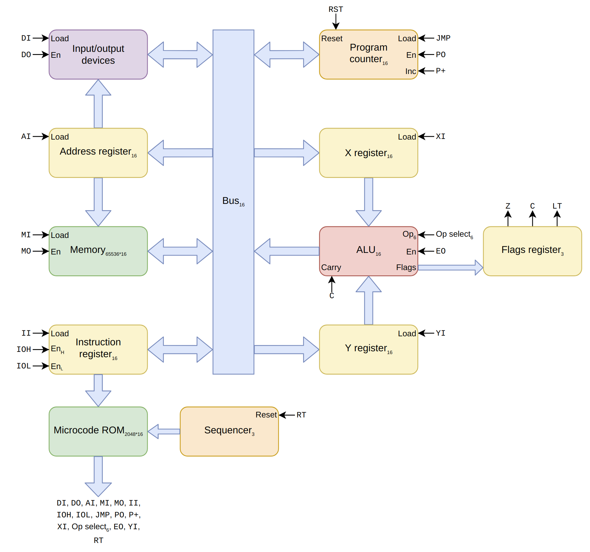
Block diagram
The diagram is roughly colour-coded to indicate parts that have similar functions. The small subscript numbers show
how many bits a register holds, or whatever else makes sense in context.
The single-width arrows carry a single bit of information. The CPU is controlled by the control bits that come out
of the microcode ROM. These are then plugged into the labels. For example, one of the control bits is AI,
which is connected to the "Load" signal of the address register. If a microinstruction enables AI, then
at the next rising edge of the clock, the address register takes on the contents of the bus.
The one thing that is kind of fudged in the diagram is that JMP just magically appears as a control signal
from the microcode, but in reality there would be some logic to combine the jump flags output by the microcode with the
flags from the flags register. I just haven't yet worked out where that logic is going to live.
Also note that while the instruction register is 16 bits wide, only 8 bits are used for the opcode, so only 8 are
used to lookup the address in the microcode ROM, which (combined with 3 bits from the sequencer) is why the microcode ROM only needs 2048 entries.
Chip counts
Here is my best guess for the number of chips I'll need for the CPU:
Module
Chips
ALU
39
Program counter
6
Instruction register
6
Control bits decoding
4
X register
2
Y register
2
Address register
2
Sequencer
2
Microcode ROM
2
Flags register
1
Total
66
In addition to this, I expect 2 chips for the RAM, 2 chips for the ROM, at least 1 in the clock, and some unknown amount more
to drive the serial ports and disk. But the whole computer will easily use fewer than 100 physical chips.
Microcode
Turning instructions into control signals was one of the things that most baffled me. Nand2Tetris
kind of glossed over this by making the instructions themselves directly set the control signals.
I found Ben Eater's 3-part video series on 8-bit CPU control logic to be superb,
it clarified everything for me.
If you have a good working knowledge of bitwise logic, but you don't quite see how it all adds up into a working
CPU, just watch those 3 videos and it will all be totally clear. I can't recommend it highly enough.
The trick is that you don't need to manually derive logic to turn instructions into control signals. You can just make a lookup table
on a ROM
that is addressed by the current opcode and the current clock cycle number, and the output of the lookup table gives you the control
signals. The contents of the ROM are called microcode. More flexible microcode
systems can keep a "micro-program counter" which is more than just "opcode + cycle count", and allow for a "micro-jump",
so that the ROM is not mostly wasted on sparsely encoding short instructions.
I currently need to generate 24 control bits, which would require 3x ROM chips if they each have 8-bit output, and if I need
even 1 more bit, then I need a 4th chip. But a lot of the control
bits don't make sense at the same time (for example I never want more than 1 module driving the bus at the same time, and I only need to
select an ALU operation if the ALU is driving the bus, otherwise I don't care what the ALU does). For this reason I came up with a simple encoding
that allows me to select all useful combinations of control bits with a microinstruction that is only 14 bits wide, which also leaves me with
2 signals spare to use for anything else I can think of.
There is more information about my control bits and microcode encoding in the doc/UCODE.md
file in my git repo.
I have also written a simple microassembler to turn microcode into hex
that will eventually be written to the ROM.
Here's example microcode that computes X = X + Y in a single cycle:
EO XI EX EY F
EO enables the ALU output on to the bus. XI enables X register input from the bus (i.e. X register gets the ALU output, in this case). EX, EY, and F select
the ALU operation (in this case: enable the X and Y inputs, and set the "function" bit, i.e. request addition instead of bitwise AND). The result
is that the current value of X and Y are enabled as inputs to the ALU, the output of the ALU comes from the adder, and the output of the ALU goes on to
the bus. So far this is purely combinational logic, and it all happens "immediately". Upon the next rising clock edge, the value from the bus (which
is X+Y) is clocked into the X register. At that point the X register takes on its new value, which then propagates through to the ALU input, and
is reflected in the new ALU output, but it is not taken into the X register until there is another rising clock edge. But before the next rising edge, there'll
be another falling edge, so we'll have a new microinstruction with potentially new control bits.
Ben Eater's CPU includes a control bit called IO which causes the instruction register to output its lower 4 bits on to the 8-bit bus,
with the upper 4 bits of the bus set to 0. In this way you can use the upper bits of the instruction to select an opcode and the lower bits to
encode an immediate small-valued constant.
I have a comparable bit called IOL which puts an immediate 8-bit constant from the low bits of the instruction register on the bus. I
also added IOH which does the same thing except with the upper 8 bits set to 1. That means IOH can be used to create immediate
constants from 0xff00 to 0xffff, which is useful for immediate small-valued negative constants, and for addresses in the top page of memory.
I propose using the top page of memory as scratch space for complicated instructions, and for a stack pointer, and for anything else that is
worth being able to access in a minimum of clock cycles. The cool part is that when using an instruction that uses an address in the
top page, you always get to pick which address it is, so for example you could use the same push instruction to handle up to 256 independent stacks.
Sequencing
The lower 3 bits of the microcode ROM address come from the 3-bit "T-state". The T-state counts up by 1 on each falling clock edge, which updates the
microcode address, which gets all the control bits set and stable ready for the next rising clock edge, at which time registers take in
new values and the program counter increments. The T-state is reset to 0 either when it wraps around after 7, or when the RT control bit is set, which allows the
microcode to finish an instruction in fewer than 8 cycles.
The first 2 T-states always have the same microcode:
T0:  PO AI    # load address from program counter
T1:  MO II P+ # load instruction register from memory, increment PC
After this, the instruction register contains the current instruction, and microcode specific to that instruction is executed. Once the instruction
is finished, it remains in the instruction register, and the next cycles tick through the first 2 states for the instruction that just executed before we
know what the next one is. So the first 2 T-states need the same microcode for every instruction, because we get the first 2 T-states
from the previous instruction's microcode.
For this reason I thought it might be worth taking the first 2 T-states out of the ROM, and letting the sequencer count up to 10, and providing
8 customisable steps of microcode per instruction instead of only 6. But I don't know that it's worth adding extra logic for.
Development techniques
I have not designed a lot of electronics before, and when I have I have basically used the Feynman
Algorithm to ensure that I had designed it correctly. Unfortunately, I'm not Richard Feynman, so it doesn't work very well, and I
normally end up getting it wrong.
For this project I have set up a development environment that is much closer to working on software than on electronics.
I am creating each part of the CPU in Verilog, and writing a testbench that checks that it works the way I expect, and then reimplementing
the part in a subset of Verilog that only uses primitives which are available in 74xx TTL chips (which I have got from Tim
Rudy). Then I can verify that the TTL implementation works the same as the high-level Verilog implementation, so that when
I finally build it out of physical chips it is guaranteed to work on the first try. How hard can it be?
The TTL-Verilog implementations of the parts are in the ttl-*.v files in the git repo. Using
a subset of Verilog that only allows for incorporation of other parts by reference, and wire connections, is basically the same as
using the HDL in the Nand2Tetris course.
My test harness is pretty janky, but does the job.
It is a shell script that uses Icarus Verilog to compile
the Verilog source into a Linux executable. Then each Verilog part has a testbench part (also implemented in Verilog) that loads the part it is testing,
drives it in various different ways, and prints out an error message if anything seems wrong. To make sure that the TTL implementation also
works, the shell script uses sed to edit the testbench source to include the TTL version of the part instead of the high-level Verilog
version, and then runs the test again.
Other stuff
It would be relatively easy to add extra functions to the ALU, selected by 1 of the unused bits from the microinstruction. My first
thought was to add an XOR function to the ALU, but it turns out that's easy enough to do with just 3 trips through the existing ALU
(x^y == (x|y) & ~(x&y)). Another obvious feature that's missing is bitwise shift. A left-shift is relatively easy
to create by composing addition (x<<1 == x+x, x<<2 == (x+x) + (x+x), etc.), but right-shift is not obviously trivial.
I expect bitwise right-shift will be particularly important for unpacking 2 bytes from 1 16-bit word. The ALU
already has native support for AND and OR, so maybe testing individual bits
would be suitable, especially if it could take advantage of a dedicated instruction for something like "test-and-set-bit":
// compute y = x>>8
int y = 0;
if (x & 0x8000) y |= 0x80;
if (x & 0x4000) y |= 0x40;
if (x & 0x2000) y |= 0x20;
if (x & 0x1000) y |= 0x10;
if (x & 0x0800) y |= 0x08;
if (x & 0x0400) y |= 0x04;
if (x & 0x0200) y |= 0x02;
if (x & 0x0100) y |= 0x01;
Currently the carry input to the ALU is always enabled, and if you don't want it you have to explicitly clear it. Clearing the carry flag
takes 1 cycle of microcode, and can't currently be done at the same time as much else as it requires the EO bit
to be set, which precludes any other module driving the bus. This means there is an incentive to
make the "with carry" version of arithmetic operations be the default one, because it saves wasting a cycle on clearing the flag.
The problem is that this is liable to turn into quite the footgun if the carry flag is ever left on by something you didn't think of,
resulting in some operations occasionally being off-by-1 by surprise.
For this reason I am considering putting an AND gate on the carry input to the ALU, with 1 of the inputs coming from the existing carry
flag, and the other coming from a currently-unused bit of the microcode instruction. That way the microinstructions that want
the carry input will explicitly enable it, and otherwise the "safety" will be on and I won't get shot in the foot.
Speaking of footguns: I thought it might be interesting to replace some of the microcode ROM with "microcode RAM". We could dedicate some portion of
the opcode space to instructions that are created at runtime! I don't even think this would take all that much logic. It would need
a single control bit that enables input from the data bus to the microcode RAM, addressed by the existing address register, and
a dedicated instruction in the microcode ROM to access it. If I wanted to dedicate half of the opcode space to this, then
I'd only need 2 extra chips to provide the microcode RAM, and 4 4-bit multiplexers that select the microinstruction from either the ROM or the RAM based
on the high bit of the instruction register. So only 6 extra chips in total. Maybe it's worth doing!
My initial objection to microcode RAM was going to be that I wouldn't want a full 50% of the opcode space to be dedicated to RAM, so
I'd need even more chips to work out whether a given instruction is backed by microcode in ROM or RAM.
But actually as long as the 128 opcodes implemented in the ROM contain enough instructions for a bootloader to work, then we can instantiate the
rest when the system boots, and just leave a small handful of opcodes free for applications to create.
I think it would be surprisingly easy to add extra registers or other modules to the CPU after it has been built (although I don't actually
expect that I will). The "bus input" and "bus output"
values from the microinstruction have a few unused encodings. I could run the control bits from these unused encodings alongside all of the bits
that are actually used, and then if I wanted to add a new register, I could just plug a new card into the bus, connect up the spare control bits, and add
some microcode to use it.
I said in the last CPU design post that I'd want to support interrupts, but having done a bit
more thinking on that I don't know if I will. I envisage running a very CP/M-like operating system on it, and polling for keyboard input
really isn't a burden for the kinds of things I'm likely to be running. The only downside of missing interrupts is that ^C won't
be able to interrupt an errant program, but in my experience that doesn't work on CP/M anyway even on machines that do support interrupts,
unless the program is already polling the keyboard.
I am currently planning to leave almost all of the internal state undefined when the CPU is reset, resetting only the program counter and
sequencer. That will mean the registers could contain arbitrary contents. I don't think this will be a problem as long as the boot ROM
doesn't make any assumptions about them.
I haven't decided yet whether the CPU will have a "backplane" that all of the other modules plug into, or whether it will be
some system of cards that have for example a female bus connector on the top and a male one on the bottom, so that they can be
stacked together.
Compared to Z80
The Z80 has separate address and data buses. To keep things simple, I only have one bus, and I have a dedicated register to
take an address from the bus and store it, to drive the address lines of the memory. The downside of only having one bus is that it
~always takes at least 2 cycles to read from memory, even if you already have the address immediately to hand in a register, because it
takes an extra cycle to load it into the address register.
On the Z80, I/O is performed by putting the I/O device address in the low 8 bits of the address bus (the upper 8 bits are ignored for I/O),
and data on the data bus. I envisage doing the same thing. I initially thought I could use the main bus to provide both the device
selection (e.g. in the upper 8 bits) and the data (e.g. in the lower 8 bits), and while this would work for output, it won't be
so easy for input, because the bus would have to be half-driven by the thing setting the I/O device selection, and half-driven by the
I/O device itself. Easier just to separate them. And having 16 bits of device selection space means I can probably just dedicate an
entire bit to selecting the device, which means I probably won't need any I/O address decoding logic.
Compared to Nand2Tetris
The main thing my CPU has in common with the Nand2Tetris CPU is the ALU. I really liked the ALU from Nand2Tetris, and have used it almost
verbatim, except I inverted the "zero X" and "zero Y" inputs to be "enable X" and "enable Y" instead. This way the X and Y inputs
can be turned into 0 using AND gates instead of multiplexers. I.e. the X input comes from X & EX instead of ZX ? 0 : X.
I didn't like that Nand2Tetris put the code in a completely separate address space to the data, and am pleased to have moved away from that.
I also didn't like that Nand2Tetris sets the control bits directly in the instruction, and I think using microcode is a definite improvement
for my purposes (although possibly not for the pedagogical purposes of the Nand2Tetris course).
Compared to Ben Eater's breadboard CPU
My CPU is very heavily influenced by Ben Eater's design. Even my block diagram is laid out in the same order as his breadboards.
The principle differences are that I am using a 16-bit bus instead of 8-bit, and I am using 16-bit addresses instead of 4-bit. Again, while
I think this is an improvement for my purposes, it is not a criticism of Ben Eater's project, which serves its pedagogical
purposes very well.
The Nand2Tetris ALU is quite a lot more flexible, and part of this flexibility gives it the ability to output either the X or Y input
unmodified (by setting the operation to addition and zeroing out the other operand). This means I can do away with the buffers that
enable the X and Y registers to be output directly on to the bus, because the same result can be achieved via the ALU, which already
has output buffers.
Operating System thoughts
I think the operating system will look something like CP/M in a Unix costume fancy-dress.
I could make CP/M support a system()-like call by swapping the currently-running
process out to disk, running the child program, and then swapping the parent back in when the child exits. We'd basically get a "process
stack", with only the top element of the stack executing at a time, instead of a traditional process tree with every element
runnable simultaneously. Starting a program would basically work like a function call.
In addition to allowing arbitrary programs to call other programs, this would also solve the biggest problem I have with CP/M, which
is that it has almost no ability to compose programs together. It still wouldn't provide a way to pipe data between concurrent
processes, because it's still not multitasking,
but you could implement simple text pipelines by having the shell run each command in order, with the output
in between buffered on disk, MS-DOS style.
In certain workflows, the system() implementation might be quite a bottleneck, so I should look at ways to optimise that: namely,
copying from memory to disk and vice versa should be done as quickly as possible, e.g. dedicated instructions to allow "output current word
to storage, increment pointer, repeat" in the minimum number of cycles.
I think I would do away with CP/M's "drive letter and user number" system for organising the filesystem, and use something much
more Unix-like, where all files exist in a single tree with directories and nested directories.