
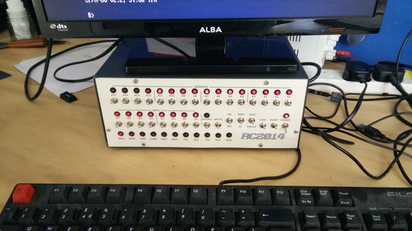
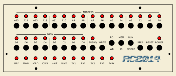
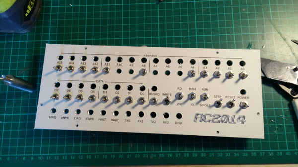
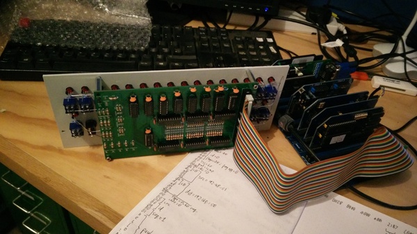
I designed and built a front panel for my RC2014. It allows you to view and alter the contents of memory, read and write to IO devices, and single-step through instructions. The RC2014 backplane basically just puts the Z80 CPU pins directly on the bus, so the same panel would work unmodified against almost any Z80-based computer, as long as you broke out the bus onto the 60-pin ribbon cable.
This is what it looks like:
And I made a video demonstrating its use:
This is a pretty long post because I want to document everything. So unless you're planning to make your own, you might prefer to just look at the pictures, and only read the parts that look interesting.
Case
Bill Buzbee used a 6U 19" rackmount enclosure for Magic-1, but that's a bit bigger than I need. I went on eBay and looked for medium-sized metal enclosures for electronics projects. There was a fair range available, but most of them were quite expensive. I ended up settling on the cheapest one I could find, which was still nearly £40.
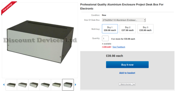
Despite being the cheapest available, I'm very happy with this case. It is made from aluminium, it has rubber feet on the bottom, vent holes on the top and bottom, all of the panels are easily removed to gain access to the insides, and it's available in a wide variety of sizes. I would like to use the same type of case in future projects.
Logic
The only reason I thought I might be remotely capable of this project in the first place is because of an excellent article in the June 1978 issue of Kilobaud Magazine. It's the one starting on page 26: "Home-Brew Z-80 System ... Part 1: front-panel construction". Incidentally, the magazine is a fascinating read just for the products that are advertised in it, even if you ignore the actual content! It includes such gems as "honestly: how many reasons do you need to make sure your next micro-processor is the original, genuine KIMTM?", and "Intertec's SuperDEC: pull out the guts & screw in the brains".

But even with the writeup in Kilobaud Magazine, I don't have a lot of experience of designing electronics, and it seemed too complicated for me to be able to get it to work. So I got rid of the auto-increment on the address bus, and just had manual switches instead. I simplified the "deposit" logic so that the automatic timing of the "write" pulse is not required, instead replacing it with a manual switch. And I used separate switches for the address and data inputs instead of using the same switches to do both. With these changes, I ended up not being able to use much of the design from the magazine, although reading it was still very instructive and I don't think I'd have even known where to start if I was on my own.
How people managed to get this stuff to work in a time before the Internet is beyond me. There's just so much to understand. And unlike software, you can't just edit and recompile if it doesn't work. You have to physically buy the components, and solder them together. It's a wonder that computers ever got off the ground in the first place.
I designed the schematic and PCBs in KiCad which is excellent software.
Reset and power
The most basic functions required of the front panel are the ability to turn the power on/off and to reset the CPU. I used a toggle switch for the power, with an indicator LED, and a momentary switch to pull the RESET line low.
BUSRQ
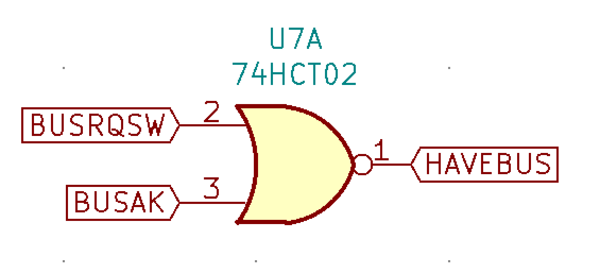
The Z80 has an active-low line called BUSRQ which is used to tell the CPU to stop what it's doing so that something else can interact with memory. When the CPU has accepted the bus request, it pulls the BUSAK line low to indicate that the bus is now available. The front panel will have a switch to let the operator pull the BUSRQ line low, and an indicator to show the state of BUSAK.
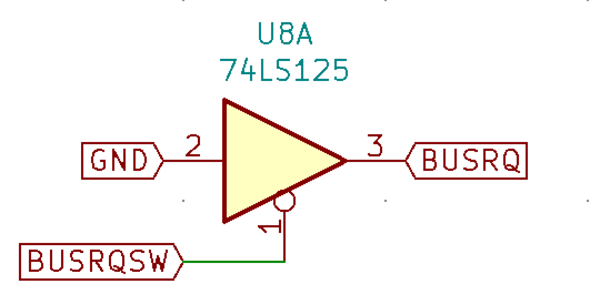
We need some logic to make sure that we only try to interact with the bus when we have asked for BUSRQ and have been given BUSAK. I called this signal "HAVEBUS". HAVEBUS is high when we have the bus. There is also "INVHAVEBUS" which is the inverse of HAVEBUS, useful for controlling active-low inputs. I used a 74LS02 quad NOR gate (there are 4 gates per chip) to generate HAVEBUS. HAVEBUS = BUSRQSW NOR BUSAK. NOR is basically AND for active-low inputs, via De Morgan's law.
(Some of the parts in the schematic say 74HCTxx but I actually used 74LSxx for everything. I don't really know what the differences are.).
BUSRQSW is the state of the BUSRQ switch on the front panel, which is distinct from the state of the BUSRQ line on the bus. Instead of connecting the switch directly to the line on the bus, it is instead used to drive a 74LS125 buffer. That way, when BUSRQSW is low, the BUSRQ line is pulled low, but when BUSRQSW is high, the BUSRQ line is left floating (it has a pull-up resistor on the CPU card on the RC2014), so that other devices can use it if they like.
Address bus
The address bus LEDs will be permanently controlled by the signals on the address bus. A pair of 74LS244 8-way buffers are used so as not to load up the bus with the current required to power the LEDs.
The address bus switches will control the bus when HAVEBUS is true, but otherwise they need to have no effect. Another pair of 74LS244 buffers are used for this, with the active-low "output enable" pins driven by the INVHAVEBUS signal.
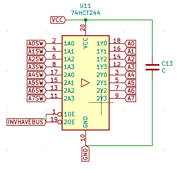
The A0SW..A15SW signals come from the switches on the panel. In one position the switch connects the signal to 0v. In the other position the switch disconnects the signal, allowing a 4k7 resistor to pull it up to 5v.
Data bus
Just like with the address bus, the data bus LEDs are permanently controlled by the signals on the databus, via a 74LS244 buffer.
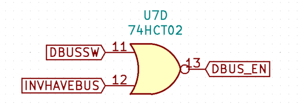
Unlike the address bus, the data bus switches only affect the data bus when we are in "writing" mode, otherwise we would never be able to read the contents of memory. The buffer that drives the data bus is activated by the "INVDBUS_EN" signal (inverse of "data bus enable"), so that it only drives the bus when the data bus switches are enabled, by another switch on the panel. Calling the switch "data bus enable" is crazy, so the actual switch ended up getting called "RD/WR", as it essentially switches between reading mode and writing mode.
Memory/IO, reading/writing
I wanted to be able to read and write to IO ports as well as memory, so a switch on the front panel lets you select between the MREQ and the IORQ pin of the bus. Just like BUSRQ, this signal is buffered through a 74LS125 so that the bus lines are left floating when they're not being asserted.
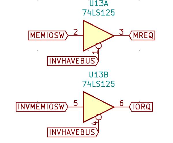
MEMIOSW is just the state of the MEM/IO switch on the front panel.
Similarly, we need to be able to switch between reading mode (which asks the memory to read out its contents, and disconnects the data bus switches) and writing mode (which connects the data bus switches to the bus, and allows usage of the WRITE switch on the panel to perform a write operation).
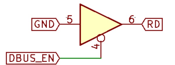
I made a logic error in driving the RD line of the bus. The DBUS_EN signal in my front panel is high when the RD/WR switch is in the WR position (i.e. we're in writing mode) and HAVEBUS is true. The 74LS125 buffer's "output enable" pin is active-low, so I drove the RD signal buffer with the inverse of DBUS_EN, so that RD would be enabled when we're not in writing mode. Unfortunately, that means that RD is enabled even when HAVEBUS is false! That means the memory is always trying to put its contents on the data bus even when the CPU is trying to write, which means the two are fighting over the contents of the data bus, some wrong bits get written to memory, and the executing code quickly goes off the rails. I only found this out later.
The WR line is driven similarly to the RD line, except with the condition that not only do we have to be in writing mode, but also the WRITE switch needs to be pressed. The reason for the separation of the writing mode (which puts the data switches on the bus) and the WRITE switch (which asserts WR) is to avoid the race condition that occurs if both happen simultaneously. When releasing WR, you need to ensure that WR is released before the contents of the data bus disappear. The project in Kilobaud magazine did this by using "one-shot" ICs to put the data switches on the bus and to trigger WR, and to make sure that the WR pulse is shorter than the data pulse, so that the write always occurs with the correct data. My solution requires less logic, and gives finer control of the bus, but means you have to manually switch between RD and WR.
Single-stepping
I copied the single-stepping logic straight out of the Kilobaud Magazine article. This is actually the part that I was most concerned about not working, because I understood it the least. For this reason, it is also the only part that I tested on a breadboard before ordering the PCBs. (Testing the entire thing on breadboards is impractical because of the number of components and connections required. I'm not Ben Eater).
This is the logic I eventually settled on:
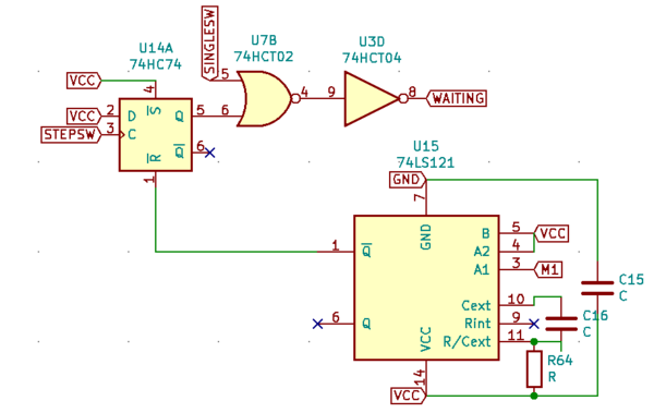
U14 is a 74LS74 D flip-flop, U15 is a 74LS121 one-shot ("monostable multivibrator"). U7 is a 74LS02 NOR gate and U3 is a 74LS04 inverter. The inputs here are STEPSW, SINGLESW, and M1. The output is WAITING, which is just used to drive a buffer to pull the WAIT line low.
SINGLESW is the switch that selects between single-step mode and the normal "run" mode. When we're in "run" mode, the WAIT line never gets asserted. STEPSW is the debounced switch that allows us to step forward by one instruction. M1 is a signal from the Z80 that goes low during the opcode fetch cycle, and is high the rest of the time.
The idea here is that when we're in single-step mode, we hold the WAIT line low most of the time. When the "step" switch is pressed, we let go of WAIT by clocking VCC into the D flip-flop via the data pin, until we see M1 go low (which means we've started the next instruction), at which point we pull WAIT low once again by sending a short low pulse to the reset pin of the D flip-flop.
When testing it on the breadboard, I originally had connected M1 directly to the reset pin of the D flip-flop and did not include the one-shot IC. This doesn't work because as soon as the CPU enters the M1 state, the reset pin of the flip-flop is held low, so pressing the step switch has no effect. The one-shot just means that the D flip-flop gets put back into a state where the STEPSW input can allow it to clock VCC in via the data pin. I was glad I tested it on a breadboard before committing to the design.
Switch debouncing
I copied the switch debouncing mechanism from the Kilobaud Magazine article. It uses dual-throw switches to activate either the "set" or "reset" pin of a 74LS279 S-R latch.
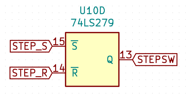
STEP_S and STEP_R are connected to opposite throws of a switch, and pulled up to 5v with a 4k7 resistor. The common pole of the switch is connected to 0v. When the switch is pressed from (say) the STEP_S position to the STEP_R position, any bouncing on the release of STEP_S, or the contact of STEP_R, has no effect, because the flip-flop maintains its state when neither of the inputs are active.
Not all of the switches need to be debounced, so most of them do not have any debouncing. For example some bouncing of the address and data switches, or the reset switch, has no ill effect.
Status lights
The only logic remaining is to generate the various status lights at the bottom of the panel.
MRD and MWR tell you when there is a memory read or write happening. Likewise, IORD and IOWR tell you when there is an IO read or write. The HALT light comes on when the CPU has halted (caused by the "halt" instruction). The WAIT light comes on when something is telling the CPU to wait. This will normally be the single-stepping logic of the front panel, but can also be caused by IO devices that need more time to handle an IO request. The TX and RX lights indicate serial line activity, and DISK indicates CompactFlash card activity.
MRD, MWR, IORD, and IOWR are made by combining the Z80's MREQ, IORQ, RD, and WR signals into a form that makes more sense to humans (e.g. MRD means MREQ and RD are both active, etc.). BUSRQ, HALT, and WAIT are taken from the bus and inverted to drive the LED because they are active-low. TX1, RX1, TX2, and RX2 are also inverted, because although the serial signals are active-high, the serial lines are in the high state when idle. The CompactFlash card activity is not a signal that is exposed on the bus so it will be provided by a jumper from the CompactFlash module.
If you're interested, you can see the entire schematic for the logic PCB here:
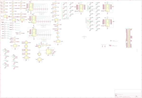
The layout of the schematic is a bit confusing, and there is also some inconsistency in the labelling regarding which of my signals are active-low and which are active-high. But it's there to look at if you want.
PCB Design
There are 3 things our logic PCB needs:
- connection to the RC2014 bus
- connection to the LEDs and switches on the front panel
- implementation of the logic
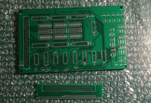
I used a 2x30 "IDC60" ribbon cable, and designed a small PCB to break out the bus on to the ribbon cable, to then carry the signals to/from the logic PCB to be mounted on the back of the front panel.
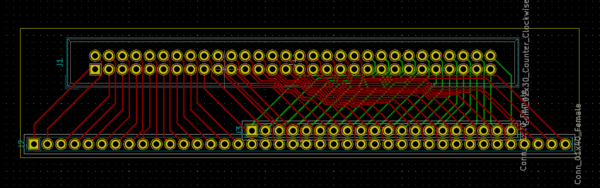
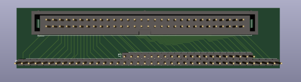
It simply connects each pin from the RC2014 bus to the corresponding pin of the IDC60 connector.
To connect to the LEDs and switches I left pads on the PCB for wires to be soldered onto. The LEDs and switches all share a common ground connection, and the remaining wire (or 2, on dual-throw switches) is to be soldered to a pad on the PCB.
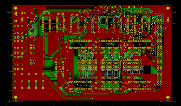
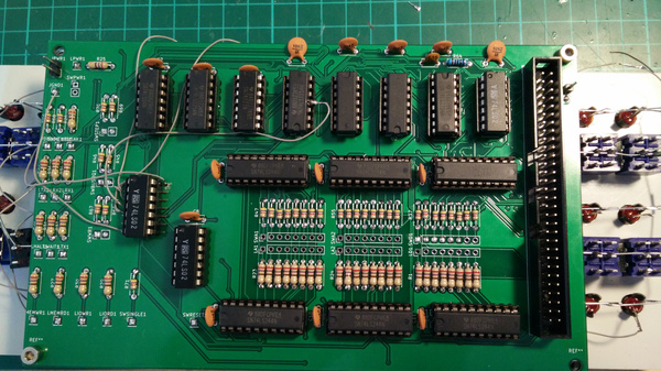
And finally, to implement the logic, I just had to position all of the components specified in the schematic, and then run traces between them. I found this difficult as there is a lot more going on on this board than on others I've done before. I started by manually spreading the components out and moving them around until the "rat's nest" looked about as simple as I could get it, and then routed traces until I was done. I made extensive use of KiCad's "push-and-shove" router here. It would have been very difficult to route everything manually. One side of the PCB has empty spaces filled with copper connected to 0v, and the other side has empty spaces filled with copper connected to 5v.
I also added a mounting hole in each corner of the PCB, to facilitate attaching it to the back of the front panel.
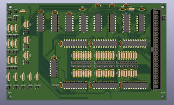
(KiCad thinks the pads for the LEDs and switches are actually pin headers, so it renders them as pin headers in the 3d view, but most of those pin headers just have wires soldered on instead in the actual build).
The 6 large ICs mounted horizontally are the 74LS244 buffers for the address/data LEDs and switches. The switch connections each have a corresponding pull-up resistor, and the LED connections each have a corresponding current-limiting resistor. There is a bypass capacitor for each IC. These are probably not necessary but can't hurt, they're just there to eliminate flakiness caused by voltage fluctuations.
I ordered these PCBs from JLCPCB, because I used them last time and was happy with the quality and price. They sprung a $5 discount on me at the checkout step, which was surprising and seems counter-productive, because I was going to buy anyway. But whatever, I'll take the discount.
Panel Design
I designed the front panel layout in Inkscape. I would have preferred to use some real parametric 2d CAD software, but I don't know anything suitable. FreeCAD's sketch editor is good, but is aimed at 3d modelling, and I don't know if you can convert the sketch into something that has text and colour and is suitable for printing. Inkscape was adequate really, but for example if you want to alter the spacing between the switches, you have to manually move every single switch which seems more like a job for the computer than the human.
(Update: Stavros points out a better way to alter the spacings: you don't have to move all the switches manually in Inkscape, you can just move the farthest two where you want them and click "align: equal spacing between").
The holes at left and right are to mount the panel to the case. These holes already existed in the panel. The 2 holes at top and 2 at bottom are to mount the PCB.
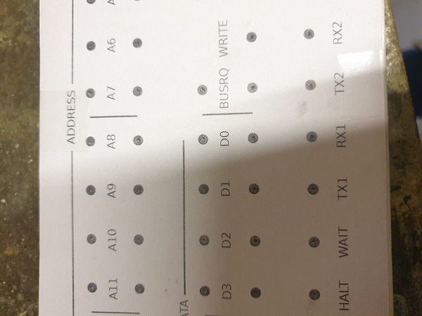
The Kilobaud Magazine article suggested that it was a bad idea to space all of the data and address switches equally, and they should instead be grouped into 3s or 4s to facilitate octal or hex data entry. I opted instead to space the switches equally, but to draw a line between the groups of 4 to visually separate them. This seems to be more than good enough. I didn't have any trouble discerning the nybble boundaries while using the switches.
I pinched the RC2014 logo from the header image on the RC2014 website and doctored it in the Gimp to make it look more reasonable against the beige background. I also kind of wanted to add one of those "Z80 Inside" logos but couldn't think of a suitable place to put it.
Panel Build
The first thing we need to do to the panel is drill holes for the LEDs, switches, and screws. I printed off a draft copy of the front panel layout, sellotaped it to the metal panel, and centre-punched all of the hole locations.
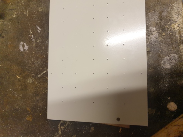
I then used these punch marks to drill a pilot hole, and then expand the holes to 7mm for the LEDs and 6mm for the switches. I didn't get the locations perfect, but they're all within about 1mm of where they need to be, which should be good enough.
I put a single LED and switch in the panel to check that they fit OK.
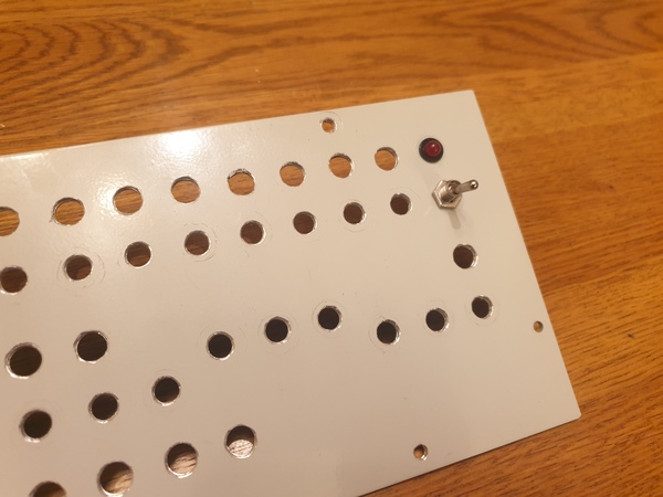
Seems fine, although I didn't like how far the switch sticks out of the panel. I solved this by 3d printing some plastic spacers to push the switch further inside.
I had ordered a high-quality print of the front panel artwork from a company called Doxdirect. I ordered it on 300gsm paper, and with a matt lamination. I was very disappointed with the quality of the lamination, it almost seemed like it wasn't laminated at all. I wouldn't get laminated prints from Doxdirect again. The quality of the actual printing is excellent, but the lamination is far too thin. I actually complained about this, and they made me another one, but the second one was exactly the same as the first.
The next job is to cut out the holes. I wasn't sure of the best way to do this. I made a cutting tool on the lathe which is basically a hollow steel rod of the correct diameter, with a sharpened end. This is based on something I remember reading in the Magic-1 build diary. I tried to use the tool by hand but it was too difficult. Ben Gazzard suggested putting it in the drill, which made it a lot easier. Once again, I didn't get all the holes in exactly the right place, but they're all close enough. Making holes in precise places is really a task for a machine, not a person.
You can see the cutting tool at the left of that photo. I did the largest holes first, then made the tool smaller to do the smaller holes. It worked OK but I think I'd put the sharpening on the outside rather than the inside if I were to do it again. It was quite hard to use because the shape on the inside tended to compress the circle of paper that was being removed, making it hard to cut all the way through.
Since there were only 6 of the smaller screw holes, I cut these carefully by hand using a knife, rather than modify the cutting tool.
With all of the LEDs and switches installed, the back of it looked like this:
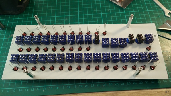
You can just about see the blue 3d printed spacers under the switches. The switches that are narrower and black are the momentary switches, that automatically spring back as soon as you let go, used for RESET, STEP, and WRITE. The panel-mount LED holders are quite good, I'd never used them before. You just push the black plastic clip into the panel, and then push the LED into the clip, and it all stays in place.
PCB Build
There's something satisfying about pristine PCBs that show up in the post, manufactured to your exact specifications, but not yet with any components soldered on.
While soldering components on the PCB I noticed a number of comical mistakes. I had placed some vias that don't connect to anything on the other side, and there are big detours in some traces that don't go around anything. The reason for this is that this is by far the most complicated PCB I've done, and routing the last few traces took me a very long time. There were a lot of false starts and undoing, with trying to get everything connected, and once it finally passed the "design rules check", I just wanted to leave it alone and not mess with it any more, so I didn't go back and clean up the mess.
After soldering all the components to the PCB I moved on to soldering on wires to the LEDs and switches. I laid the front panel and the PCB both upside down, next to each other, and ran the wires across, so that the two halves can then be "folded" together to form the complete assembly.
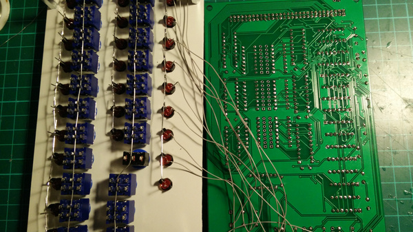
You can see in that picture that I've soldered some of the wires for the status lights, and I've also connected all of the ground connections of the LEDs and switches together. I did this for the LEDs by bending the negative leg to reach the adjacent LED and then soldering them together, and I ran a piece of uninsulated wire along each row of switches.
Soldering the wires to the LEDs was quite difficult owing to my unfortunate disability: I only have 2 working hands. Instead of trying to hold the wire, solder, and soldering iron simultaneously, I first put a blob of solder on the leg of the LED, and then re-melted the blob while poking the wire into it. It worked OK but it was quite time-consuming and they're not particularly good joints. The switches were easier as they have holes on the pins that do a good enough job of keeping hold of the wire.
With the first few LEDs wired up, I plugged in the ribbon cable and tried to switch the computer on to verify that they flash as expected.
The lights that were connected did flash as expected, but the computer didn't actually work. This was puzzling. I assumed that some of the logic must be in a wrong state due to the unconnected switches, so I went and connected the important switches and tried again. It still didn't work.
Blunder 1
For a quick sanity check, I ran my finger across all of the ICs and noticed that one in particular was very hot! I immediately switched the computer off and took a better look. I'd plugged it in upside down. D'oh! You can just about see the mistake in the picture above. It's the top-right IC, and you can see that the notch drawn on the silkscreen is not matched with a notch on the actual chip. An interesting property of the 74xx series logic chips is that the ground and +5v connections are at opposite corners, so if you accidentally plug the chip in backwards it is directly reverse-biased. I don't know if this is helpful because it alerts you to the error quickly, or harmful because it is likely to damage the chip.
I took the chip out and replaced it with another one (I was worried it might be broken and didn't want to take any chances, although it turns out the chip still works fine). But the computer still didn't work.
Blunder 2
Nothing else was getting hot, and I couldn't spot any other mistakes, so this had me scratching my head for quite a while.
Eventually I removed the ribbon cable and verified that the computer still worked without the front panel attached. It did.
I then connected signal lines from the bus to the front panel individually using jumper wires, one by one, until the computer no longer worked, and I discovered that it worked as long as the RD line was not connected to the front panel. I had a good look at the PCB and still couldn't see any mistakes. All the pins were soldered correctly, and there were no solder bridges.
So then I went back to the schematic to see if I could figure out what was wrong, and realised the mistake almost straight away. It was the logic error described earlier, where RD was always held low when we're not writing, even when the front panel doesn't have control of the bus. D'oh!
The solution here is to modify the circuit to use a NOR gate and an inverter so that the RD line is left floating when either we're in writing mode, or we don't have the bus at all. While not all of the gates of all of the chips on the board were in use, it turned out I had no spare NOR gates and no spare inverters. I really didn't want to have to pay for (and wait for) a new PCB, so I considered various ways to add a chip to the existing PCB. Eventually I settled on supergluing an IC socket to the board, with the pins bent outwards, and then running wires from these pins to the various places they need to connect to.
Note the leftmost chip, with the grey wires running to it.
I thought this was quite an elegant fix, all things considered. There are just a handful of bodge wires running around the board to connect the new chip up to the signals it needs, and I bent out the pin that it needs to drive on the chip that was already there, so that pin is no longer driven by the offending signal on the PCB.
I connected it back up to the RC2014 and the computer now worked! That was a relief. I soldered up most of the rest of the LEDs and switches, and found that everything worked. Great success.
The only thing left is to wire up the power switch (easy) and the "busy" light from the CompactFlash module.
Blunder 3
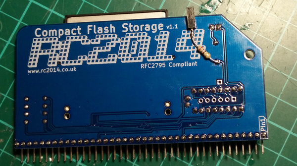
The RC2014 CompactFlash module already has an LED on it to indicate when it is busy, so my plan was to simply break this signal out to a pin header socket superglued to the card, and then run a wire from the pin header socket over to the pin header on the front panel PCB. There's no resistor for it on the front panel PCB, so I added that on the CompactFlash module as well.
I thought this was definitely going to work and couldn't even imagine how it could go wrong. The power to the LED is just copied over to the front panel. What could be simpler?
Well, I plugged it all in and found that the DISK light on the front panel stayed lit 100% of the time. It turns out that the LED on the CompactFlash module is switched on the negative side rather than the positive side, so the positive side is always at 5v. D'oh! I didn't fancy the idea of solving this by dismantling the front panel assembly and rejigging the soldering on the DISK light, so I instead used the switched-ground signal on the CF module to switch an S9015 PNP transistor that would then switch a positive supply to the DISK light, and that worked.
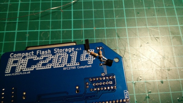
Not as elegant as what I had in mind, but it does the job.
Assembly
The logic PCB attaches to the back of the front panel with 4 long standoffs. They're pieces of hex bar that are threaded to M3 all the way through. Each one has an allen bolt at the front to hold the front panel to the standoff, and an allen bolt at the back to hold the PCB to the standoff. It's a very quick and easy way to attach flat panels together at a fixed distance.
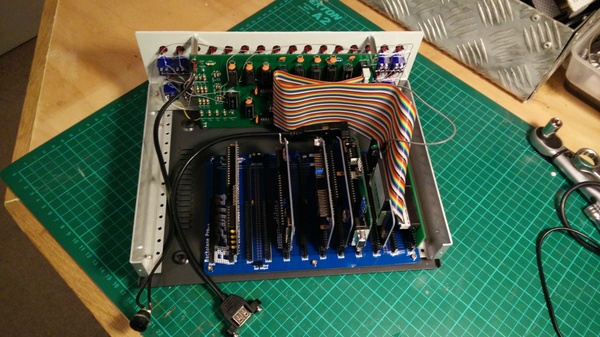
To screw the backplane into the case, I removed all of the cards and used the backplane mounting holes as a drilling template to put 6 holes in the bottom of the case. I then bolted some short standoffs to the bottom of the case, and attached the backplane to the standoffs with short allen bolts.
An unfortunate consequence of the bus-to-IDC60 break out board is that it essentially takes up 2 backplane slots just because the ribbon cable sticks out too far to allow access to the adjacent slot. An improvement would be to use a 90-degree IDC connector so that the ribbon cable plugs straight down instead of from the side.
To get power to the computer I've wired up a panel-mount barrel jack socket to a cable with a pin header socket on the other end. The pin header socket plugs into a pin header on the logic PCB (with the positive side coloured red so that I don't install it backwards) and will eventually mount in the back panel of the case.
The USB keyboard input to the VGA serial terminal is in an inconvenient place, so that too has a cable to bring it round to a panel-mount connector.
The only other connections I need are the VGA connection and the second serial port. Both of these are positioned on cards close to the back of the computer already, so I'll probably just cut holes in the back panel that are large enough to provide access.
Power supplies have come on quite considerably since the late 70s. Small, cheap, and efficient DC switch-mode power supplies are today so abundant that we don't even notice them, but the Altair 8800 used a power supply that was almost as big as the rest of the computer put together!
Not only is such a linear power supply large and expensive, it is also quite inefficient, wasting a lot of power and heat, and necessitating a large fan to keep it cool. I considered adding a small fan to the inside of my case, but nothing here gets noticeably warmer than ambient temperature. The fan would really only be there for sound effects, which doesn't seem worth it.
Usage
I hand-assembled a short program using the clrhome.org Z80 instruction set table as a reference. It's a very good presentation of the instruction set, showing all 1-byte opcodes on a single screen, and giving more information about each one on mouse hover, with multi-byte opcodes further available down the page.
Having generated the machine code, we need to get it into the memory so that the machine can execute it.
Unfortunately, when my RC2014 is reset, it maps a ROM bank at address 0, and it is not possible, with my front panel, to interrupt the CPU before it has fetched the first opcode. But the first instruction in the ROM is a jump. The easiest way I have found to execute a program using the switches is to grab the bus after the CPU has fetched the jump opcode, and then switch in a RAM bank at address 0, and then toggle in the destination address for the jump (i.e. write 0003h - but little-endian - to send execution to address 3), followed by the actual code to execute, starting at address 3. When the bus is released and the CPU continues executing, it has already fetched the jump opcode from address 0 of the ROM, and it proceeds to fetch the destination address from addresses 1 and 2, which then point to address 3, and we've hijacked the ROM's jump to instead jump to our own code in RAM.
The bank switching is quite simple, but not obviously documented anywhere. I worked out how to use it by finding the relevant config in the RomWBW source. You first have to write a 1 to IO port 0x7c to enable paging, followed by writing your bank selection number to IO port 0x78, 0x79, 0x7a, or 0x7b, depending on which page you want to switch. Each page is 16K long, and can point to one of 32 available ROM banks, or 32 RAM banks. The page for addresses 0000 to 3fff is switched using IO port 0x78. Bank numbers 0 to 31 are ROM, and 32 to 63 are RAM, so to put a RAM bank in the first page, I write a 32 (0x20) to IO port 0x78. An interesting property of the bank switching is that you can have multiple pages pointing to the same bank at the same time. For example if you write the same bank number to IO ports 0x78 and 0x79, then every byte in the range 0000-3fff will be the same as the corresponding byte in the range 4000-7fff.
For extended front panel usage, it would be worth removing the 512K ROM/512K RAM card and replacing it with a single RAM chip connected directly to the bus, with no bank switching logic. That way you'd just toggle in the code starting at address 0 and hit reset.
I originally wanted to narrate the video demonstration to explain what I'm doing, but I felt quite strange sitting on my own narrating my actions, so I stayed quiet and added textual annotations instead. They're probably more useful anyway.
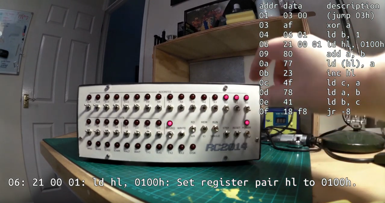
At about 1m28s in the video you might notice that the A1 light flickers while I'm not touching the switch. The toggle switch on the A1 line is a little bit flakey, but it seems to be getting better with use so I expect it just needs to wear in a little bit. At any rate, it's not bad enough to be worth dismantling the whole thing and replacing the switch.
Having to manually toggle in every single address is much more work than I anticipated. I can certainly see why most front-panel-oriented computers have an auto-increment feature for the address.
Something I wasn't sure about was whether it is safe to switch the clock speed selection jumper while the computer is running, if the CPU is blocked on either BUSRQ or WAIT (from single-stepping). I tried it and it works fine, which is quite handy.
Anyway, that's all I have to say about my front panel project. I learnt a lot about electronics and computers, and enjoyed the process. Please email me if there's more you want to know about it, or if you're thinking of making your own front panel.
More
I still need to make some holes in the back panel of the case to mount a power socket and USB keyboard socket on, and allow access to the VGA and serial ports.
I'm planning to eventually be able to use the serial port for SLIP networking. I have a basic ping test working in CP/M, but nothing more. It takes 900ms to reply to ping, or 80ms if debugging prints are removed. I'm writing the code in ZDE 1.6 which is not good but is better than ED. And I'm using the Hi-Tech C compiler to compile it. The Hi-Tech C compiler is seriously old. Hailing from 1987, it pre-dates even C89!
I'd like to find a better text editor. ZDE is much better than ED, but it still sucks. David Given wrote a vi implementation for CP/M in a 9-hour live stream, but it is targeted at his Kaypro II terminal and I tried it briefly but it didn't quite work right with the RC2014 VGA serial terminal, so I think it would need some modification.
Another thing I'd like to make is a basic sound card. There are a handful available for the RC2014 using commercial sound chips, but I'd like to do it from first principles instead. It would probably just be able to output a single tone, like a PC speaker, rather than arbitrary sounds like a proper sound card. For example using some glue logic to let the software write a frequency selection into an IO port, which then controls a square wave generator circuit of some sort. You could conceivably include more than one on the same card (at different IO ports) to allow multiple simultaneous tones.