
I'm going to get most of the PCBs for SCAMP made by JLCPCB, but I'd like to try to mill the backplane on the CNC machine because it is both large (expensive at JLCPCB) and simple (single-sided, no vias, easy to make). Yesterday some small pieces of copper-clad board arrived and today I had a first attempt to see what would go wrong.
This is what I got:
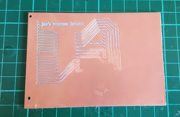
It's meant to be an EEPROM burner (how did you guess?), but obviously this one is not going to work. It doesn't look far off though, I think the PCB milling process is going to work.
Principle
Start with a copper-clad FR-4 board. This is a fibreglass board with a thin layer of copper on one side. This is the normal type of board that a single-sided PCB is made from. Double-sided PCBs use the same stuff, but with copper on both sides.
Using a very fine cutting tool, cut out the copper around the edges of the areas that you want to conduct, so that the conductors are isolated from one another, also called "isolation routing" or "isolation milling". You're left with a board that is functionally equivalent to an etched PCB, but for a fraction of the effort.
In theory you can do double-sided boards if you're careful about alignment when flipping the board over, but you don't get plated-through-holes, which means you need to be cognizant of which side components are soldered to (because they won't be connected to the other side), and you need to manually put a bit of wire or something inside vias, and unless you can use a very small drill bit, your vias have to be quite a bit bigger than normal.
For my case, on single-sided boards, the main downsides compared to a professionally-manufactured PCB are that trace width and clearance need to be larger, and there's no solder mask and no silkscreen. The benefits are the quicker turnaround time compared to waiting for a board to be shipped from China, and the obvious cost saving.
PCB design
The EEPROM burner design looks like this:
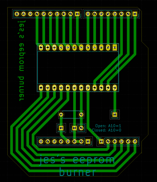
It's meant to sit on top of an Arduino Uno and hold a ZIF socket so that I can program the EEPROMs. Unfortunately the Uno is 1 GPIO pin short of what I needed, so there is a jumper that allows me to manually select the high address bit. That's annoying but I don't plan to have to use it very often. A better solution would be to use something like an MCP23017 port expander to let the Arduino drive more pins than it physically has.
I didn't make a schematic for the board, I manually laid it out directly in Pcbnew.
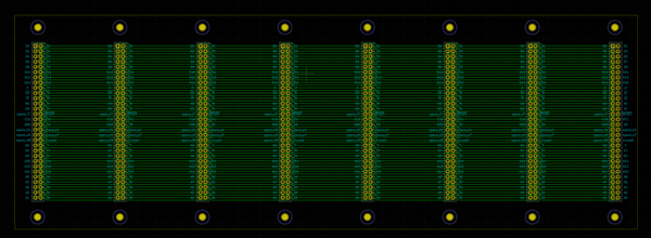
The backplane PCB layout is only slightly more difficult, mainly because it needs to route traces in between pads, which means the traces need to be narrower and closer together:
gbr2ngc
I tried using pcb2gcode and FlatCAM, but couldn't get either of them to build and run successfully.
I then found gbr2ngc, "Open source no frills Gerber to gcode converter", which does precisely what I wanted and no more, and it builds and runs easily. Great success.
I did find that since I wanted copper on the bottom of the board instead of the top, it generated the G-code as if it was looking directly through the PCB, and I needed to invert the Y coordinates separately. I added a --invert-y option to gcodetile to do this for me, and strung everything together with a little shell script.
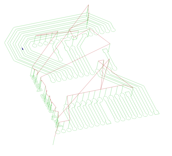
The G-code paths for the copper cuts look like this:
drl2gcode
Converting Gerbers to G-code is only half the story: we also want to automate the hole drilling.
I found drl2gcode on nexlab's gitlab instance. It does almost exactly what I want, but it generated G-code that wasn't quite right for my machine, and took configuration parameters as globals instead of command-line options, so I made some changes that were more to my taste.
argparse
Incidentally, I found the Python argparse documentation to be surprisingly obtuse. It includes a confusing example of a command-line switch that changes a parameter from pointing at the max() function to make it point at the sum() function, but it does not include an example of how to take a named numeric argument, like --spindle-speed 10000. I just guessed a few variations until it worked.
Here's the Python argparse example usage:
import argparse
parser = argparse.ArgumentParser(description='Process some integers.')
parser.add_argument('integers', metavar='N', type=int, nargs='+',
                    help='an integer for the accumulator')
parser.add_argument('--sum', dest='accumulate', action='store_const',
                    const=sum, default=max,
                    help='sum the integers (default: find the max)')
args = parser.parse_args()
print(args.accumulate(args.integers))
And here's the Perl Getopt::Long example usage:
use Getopt::Long;
my $data   = "file.dat";
my $length = 24;
my $verbose;
GetOptions ("length=i" => \$length,    # numeric
            "file=s"   => \$data,      # string
            "verbose"  => \$verbose)   # flag
or die("Error in command line arguments\n");
Maybe I'm biased, but I know which one makes more sense to me.
Cutting copper
Having generated my G-code, I went out to the garage armed with a USB stick, a copper-clad board, and a cup of tea. I arrived to find the room at 0°C, which is less than I prefer.
I stuck the copper-clad board to the bed with double-sided tape. I'm not sure if this would be enough to hold it for the edge cuts, but it's more than adequate for the isolation routing.
Here's the picture of the board again:
The problem here is that the top surface of the copper was not perpendicular to the Z axis of the machine, which means the cuts are too deep in some areas and not deep enough in others. Here's an exaggerated example of a constant cut depth against a part that is not perpendicular to Z:

Tool geometry
But we actually only really care about cut width, not depth. As long as we are cutting the copper away, and not cutting all the way out the other side of the board, we only care about cut depth to the extent that the cut width varies with depth. We can mitigate this problem by using a steeper tool:

The steeper tool causes less width variation as the cutting depth varies. The ideal case would be an extremely thin tool with straight sides (i.e. an extremely narrow end mill), but I think a ~0.1 mm end mill would be too fragile.
I am still awaiting delivery of a 10° engraving tool, so today I used a small 60° engraving tool that I already had.
Bed surfacing
I use an MDF wasteboard on my bed, and part of the reason that the cut depth is not uniform is because my wasteboard has been cut up a bit, which means the surface of the wasteboard is no longer flat. I would probably get a substantial improvement from re-surfacing it, which just involves running a large cutter back and forth over the entire surface at a fixed height.
Mesh leveling
A more general solution is to probe the height across the entire board before we start milling, and then offset the Z coordinate at each point by the probed Z coordinate from the bed:
(Thumbnail from this video.)
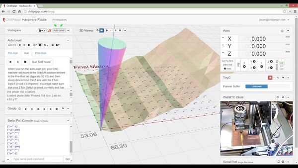
UGS Platform includes a plugin to do this, but I loaded it up and it popped up a box saying that it doesn't work correctly, so I didn't risk it. I will probably try out the plugin at some point, but failing that, it would not be too hard to write a program to do mesh leveling myself:
- probe the Z height in a grid that covers the part
- export the measured Z heights in a text file
- read in the G-code for the part and adjust each Z coordinate by the corresponding (interpolated) Z height from the probe data
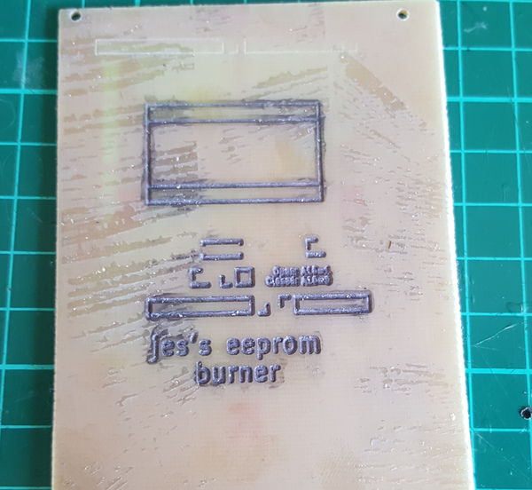
Cutting silkscreen
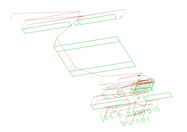
Silkscreen is not really important for the EEPROM burner, but I'm keen to be able to put writing on the backplane so that I can label the signals, so I thought I'd test it out on the EEPROM burner.
There are a few things here.
Firstly the horrible sticky residue is from the double-sided tape that I used to stick the board down when cutting the copper side. Normally the tape peels off easily without any residue left behind, but I think it doesn't like the cold. Hopefully it will be warmer next time, if not I might heat the board up before peeling the tape off. If that doesn't help, then it might be that the tape sticks to FR-4 much better than it sticks to aluminium, and I'll have to think of something else. Maybe just dissolve it with isopropyl alcohol.
The second thing is that the cuts are very deep. They are much deeper than necessary, because the cut depth is not really critical and I couldn't be bothered trying to set it up precisely, but it makes the small text quite hard to read, so next time I'll try to do better.
The third thing (masked by the excessive cut depth) is that gbr2ngc has actually tried to isolation-route this layer, i.e. it has tried to cut around the outside of the letters, instead of cutting the letters directly. That's not a big problem, and I don't think I'll try to fix it.
To make the writing stand out a bit, I traced over the cuts with a Sharpie and then tried to rub off the excess. It mostly worked, and I might stick with this method, mainly the sticky residue made it hard to rub off the excess. Another idea I've had is to spraypaint the board black before making the cuts, so then the cuts will be fibreglass-coloured and the rest of the board will be black. Might be less work because I don't need to manually go over every cut, and I don't need to rub off the excess.
The small writing is kind of hard to read, but I expect this will be improved by using a steeper cutting tool and setting the depth more precisely.
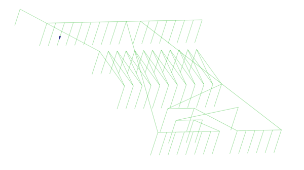
The path I used looks like this:
If you zoom in you'll see that each line is actually 2 lines spaced very slightly apart.
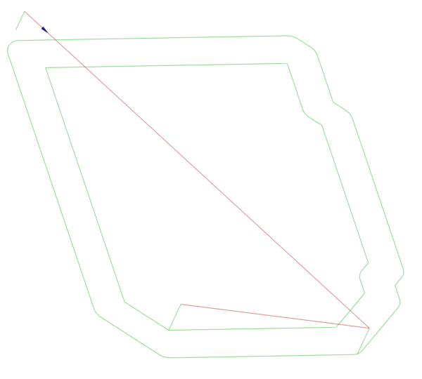
Drilling
I didn't run the G-code for drilling the holes because my 1 mm drill bit has not arrived yet, and I didn't see that it would be much use drilling it a different size since the PCB obviously isn't going to work anyway. The path looks like this:
For next time I will invert the Y coordinate of the drilling path so that it can be done while the board is still upside down, that way if there's any misalignment when the board is flipped over for the silkscreen, at least the holes will still be in the right place.
Edge cuts
I also didn't run the G-code for making the edge cuts, although in hindsight I should have done, to find out whether the sticky tape would be sufficient to hold the PCB. The path looks like this:
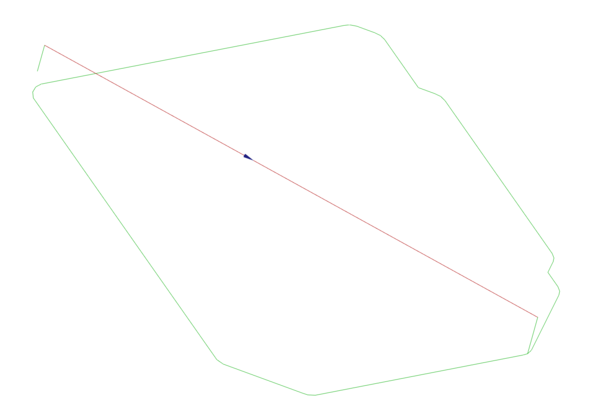
grb2ngc initially generated a path like this:
Because it views the "edge cuts" as if they are copper traces that want to be isolation routed. The generated G-code is neatly labelled in 2 paths, though, so it's easy to get rid of the second one with sed.
Next attempt
I plan to:
- use a 10° cutting tool instead of 60°
- re-surface the wasteboard
- work out how to do mesh leveling
- use a more precise cut depth on silkscreen
- invert Y coordinate for drill G-code
- try out the drill and edge cut G-code
- heat the board up before peeling the tape off if it's cold
And hopefully that will be enough to get a working PCB.