
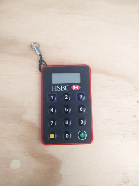
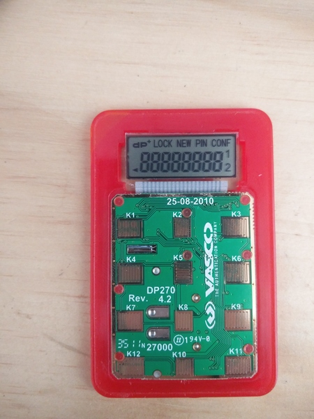
You've probably seen an HSBC SecureKey. It's a 2-factor authentication device for online banking. I was given one because the previous owner had started using the bank's smartphone app and no longer needed the SecureKey. It looks like this:
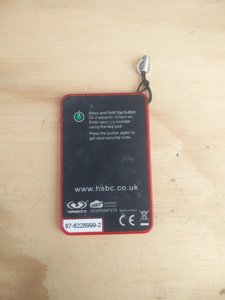
I'm not sure if the numbers on the bottom left of the case back are sensitive. I surmise that they must not be sensitive, otherwise that would transform the 2FA device from "something you have" into merely "something you know". If the numbers are sensitive, please let me know rather than using them for evil :).
The red stuff around the edges is a plastic case. With no obvious seam, I thought the case halves must be ultrasonically welded together to prevent tampering.
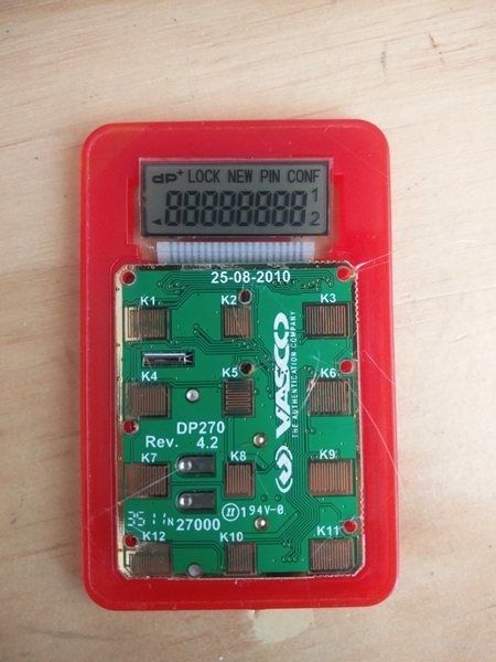
I peeled off the front and back stickers to see what we're working with.
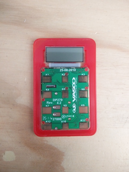
The "case" is not a clamshell at all! It's just a one-piece skeleton that everything is attached to. The insides are only separated from the outside by the stickers.
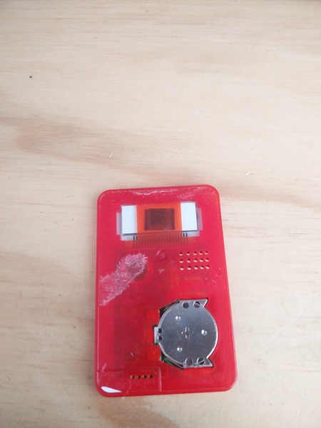
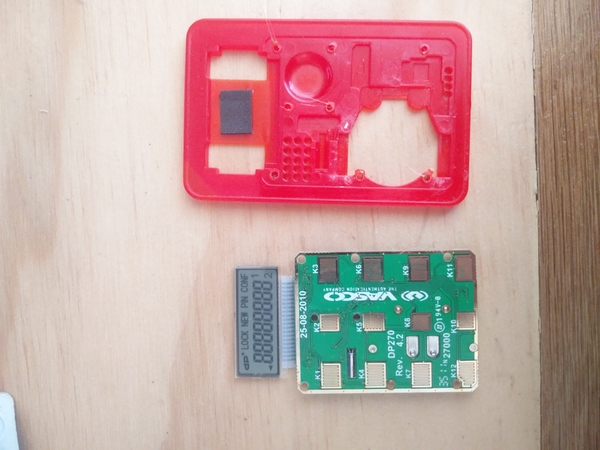
There are some interesting holes in the back of the case, with some gold-coloured stuff underneath, but at this point I couldn't work out what they were for.
The PCB has some holes in it, and some plastic from the case has been smooshed (?) around the holes to retain the PCB. I tried to remove the board by prying at it with a knife, but it was retained quite well and I think I must have broken something:
Pressing the buttons no longer has any effect, it just lights (darks?) every cell of the LCD and does nothing else.
So for my next trick I used a hot soldering iron to remove the smooshed bits of plastic:
(with the battery still in place, you understand, because it can't be removed until the board is removed from the case)
And then prying the board out with a knife was much more successful.
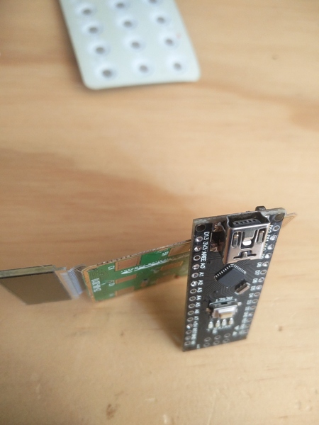
The case has some cutouts in it for the components that are mounted on the board, presumably to keep the device as thin as possible. The circuit board is also extremely thin. This is probably why I damaged it so easily when prying at it earlier. It is about 0.5mm thick, or about 2 moustache hair's diameters.
Here it is compared to an Arduino Nano, which weighs in at nearly 2mm:
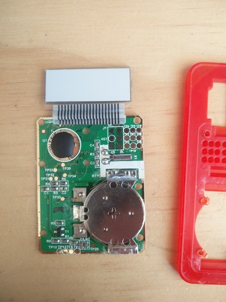
Back to the interesting side of the circuit board:
The traces are gold-plated, which is a surprise. Possibly to help conductivity because they're so thin. Apart from that, there's almost nothing to see here. The battery takes up over a quarter of the board. There are a handful of resistors and capacitors. One transistor. A crystal oscillator. And a bunch of exposed gold-plated pads, mostly labelled "TPxx". These are "test points", and they line up with the holes in the plastic case, so that explains what the holes were for.
The 2x3 grid of pads near the middle is likely to be for JTAG access. If I knew how to communicate with (over?) JTAG (and if I hadn't broken the board earlier) it might have been interesting to play with this.
So the only thing left is the epoxy-topped "chip on board". This is a bare silicon die placed directly on the board, without any packaging, and then epoxied in place. It would be interesting to look inside.
I've never decapped a chip before, but there's a first time for everything. I tried to read up on how to do it and it mostly involved scary talk of very strong acids which I didn't like the sound of. I eventually found this video wherein Kai Bader decaps an IC with just a heat gun and a scalpel. Unlike using acid, this process destroys the bond wires (and probably scratches up the die too much) so the chip will never be made to work again, unless you're a wizard. But I was under no delusions about that anyway.
I found it more convenient to use a soldering iron than a heat gun, but the process went much the same as depicted in Kai's video. Just keep heating and cutting and scraping until the die is fully exposed.
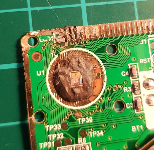
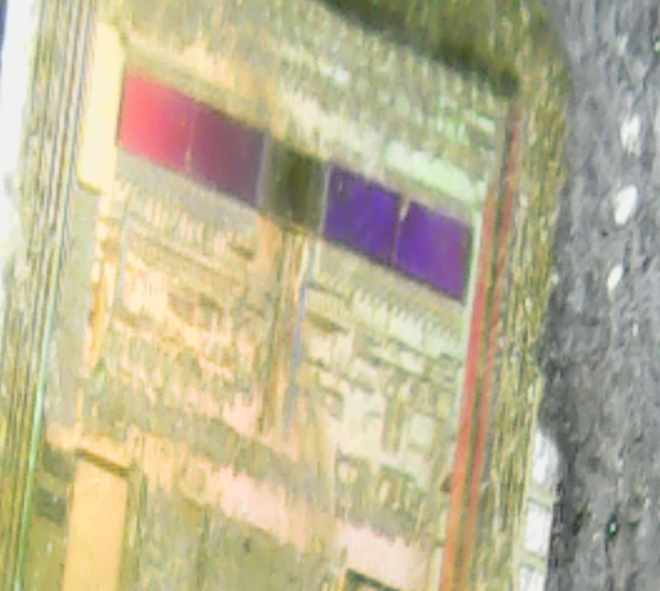
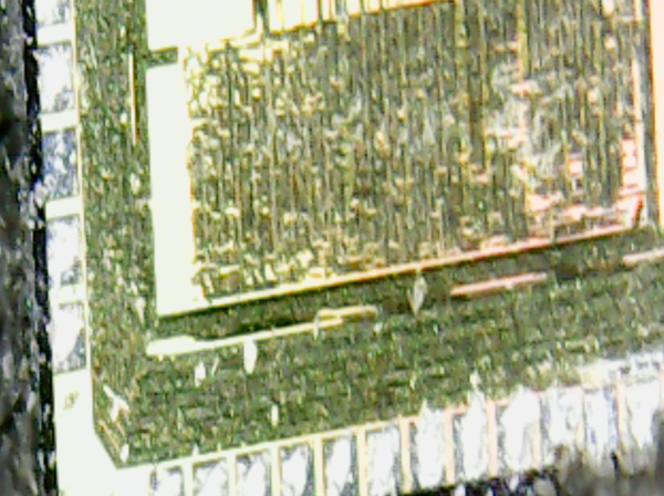
You can see a surprising amount of detail on the die using just the camera from a smartphone. It's nowhere near ZeptoBars level, but it's a better start than I expected.
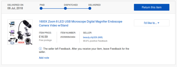
It would be cool to get a more detailed shot than this, so I went on eBay and bought myself a "1600X Zoom 8 LED USB Microscope Digital Magnifier Endoscope Camera Video w/Stand" from a seller called "beauty.city329". The "1600X" turned out to be optimistic by a factor of at least 100.
I crossed my fingers and tried to get Linux to understand how to talk to it, and surprisingly got it working quite quickly. (I just had to install a couple of packages from apt, but I can't quite remember what they were.)
This is what my setup looked like:
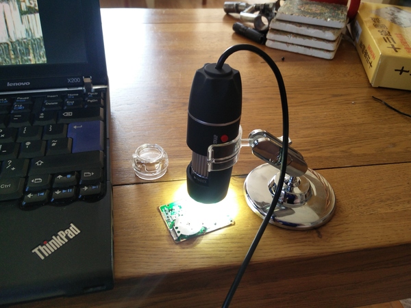
I took the clear lens cover off because it was preventing the lens from getting close enough to the die.
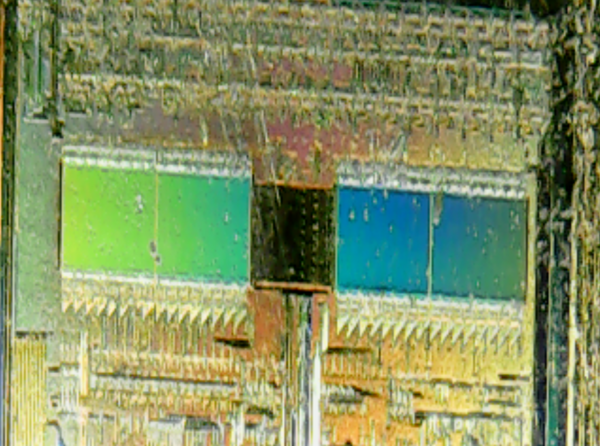
The USB microscope focuses on a very small area (especially at zoom levels nearing the heady heights of 16x...) so it was quite difficult to position the die in the frame properly. It was also quite difficult to focus the image since the microscope has an extremely short focal length, although it thankfully does have a manual focus. This is the first picture I managed to get:
It's a little bit more detailed than the smartphone managed to get, but... not much more detailed. I don't know whether this says more about cheap smartphone cameras or about cheap USB microscopes.
I played around for some time and took a handful more pictures of the die:
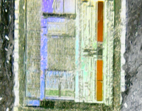
The 2 green parts in the first picture are the same part as the 2 orange parts in the second picture (the colours change as the light changes). The aspect ratio of the camera in the microscope is clearly not very accurate.
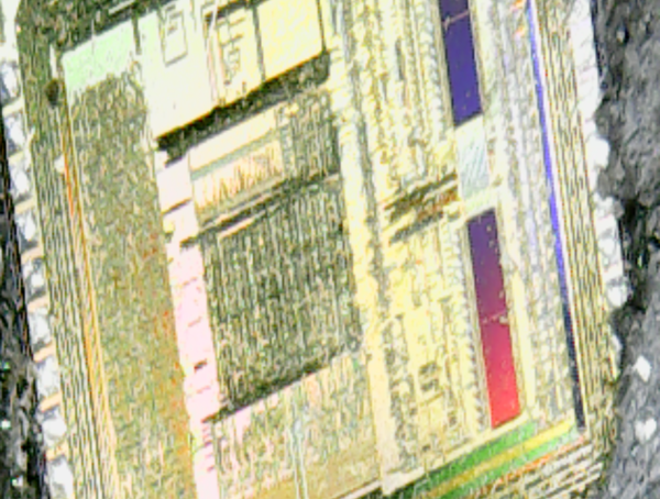
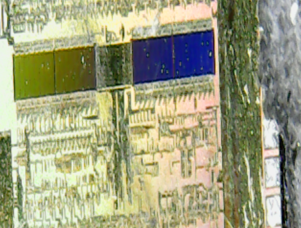
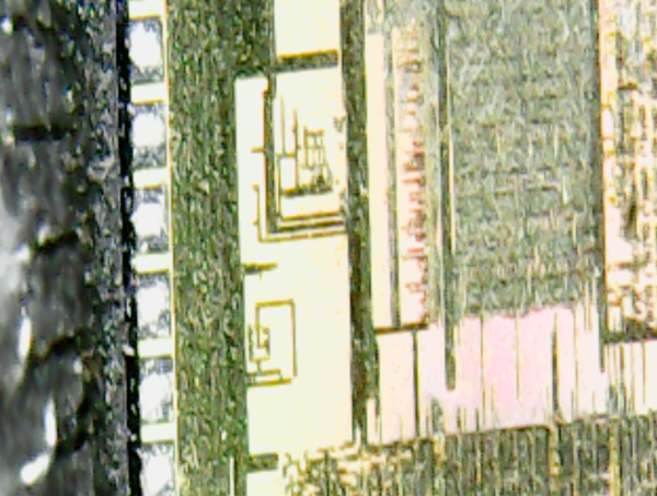
Not really enough detail to make anything out (at least, not to my untrained eye). Somebody who knows more about integrated circuits might be able to identify the 2 large rectangles, I suspect they're memory of some sort.
Anyway, there we have it. That's what's inside an HSBC SecureKey.